PRODUCTS

- Home
- Products
- 3D Morphology
- 3D Surface Topography Measurement Platform

3D Morphology
3D Surface Topography Measurement Platform
- Features
- Non-contact, high-precision 3D surface topography measurement
- Wide field of view and high-efficiency scanning capability
- Compatible with diverse materials and surface conditions
- Rich analysis of surface morphology and feature characteristics
- Modular hardware/software with open expansion interfaces
- High stability design with vibration resistance
- Broad applications across multiple industries:
- Wafer manufacturing: TTV / Bow / warpage monitoring for process optimization
- Glass stacks (GoG/GoP): thickness and flatness inspection
- Printed Circuit Boards (PCB): thickness distribution, warpage, and solder pad inspection
- Exterior and stamped components: dimensional accuracy, edge/hole precision, and assembly tolerance
- Coatings: uniformity, step height, and local defect evaluation
- Gears and mechanical parts: tooth profile accuracy, 3D contour, and wear analysis
- Prototype assemblies: gap/interference prediction and risk assessment
- Incoming/outgoing inspection: ensuring supply chain consistency
- R&D DOE: correlation of surface metrics with functional performance and reliability
- Automotive displays & consumer optics/structural parts: mass production quality control
3D Surface Topography Measurement Platform
Thickness, Warpage & Flatness|Point Cloud Analysis & CAD Comparison
Platform Overview
Our platform integrates Color ConfocalNon-Contact 3D ReconstructionPoint Cloud/Mesh AnalysisCAD Comparison and Statistical Evaluation. It delivers thickness, warpage, TTV, Bow, flatness, edge geometry, and more for glass, silicon wafers, and multilayer structures.
- Automated workflow: recipe-driven measurement, batch processing, report generation
- Versatility: handles glossy/matte, transparent/semi-transparent, reflective/rough surfaces
- Semiconductor-friendly: wafer-map visualization, TTV/Bow/warpage statistics
- Traceability: standard reference calibration, measurement uncertainty, version control
Color Confocal Thickness & Warpage Measurement
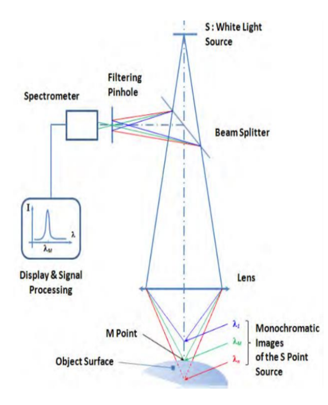
- Optimized for glass and silicon substrates
- Thickness measurement range up to 0.7 mm (extendable with optical options)
- Accuracy < 2 μm; repeatability < 2 μm (sample- and environment-dependent)
- Supports multi-point thickness distribution, warpage/flatness analysis, wafer-map output

Note: accuracy/repeatability are influenced by surface condition, fixturing, vibration, and temperature drift. Trial runs are recommended for parameter optimization.
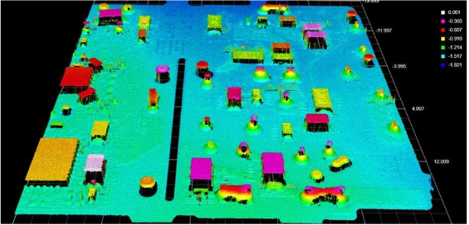
iboson 3D Data Analysis
Our toolchain covers point cloud cleaning, meshing, surface reconstruction, and GD&T dimensional analysis. It supports CAD comparison, error heat maps, best-fit alignment, and statistical reporting. Recipes ensure repeatability across large sample sets.
- Filtering and resampling (denoise, hole filling, outlier suppression)
- CAD alignment and deviation analysis (global/local registration with distance mapping)
- Statistical metrics: mean/median/percentile, Cp/Cpk, yield indices
- Version control: recipe versions and results tracking for audits


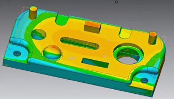
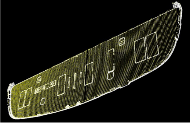
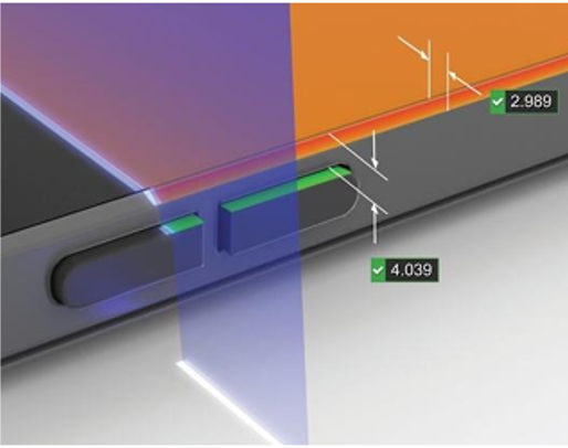
Non-Contact 3D Surface Reconstruction
- Handles glossy and matte surfaces
- Supports high-precision dimensional and GD&T analysis
- Multi-layer thickness, step height, and local surface evaluation
- Flatness, assembly tolerance, and fitting assessment
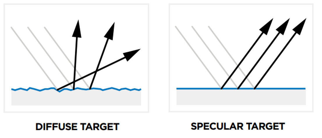
Methods Comparison
Different techniques have unique strengths across feature size, surface type, transparency, and throughput. The table below provides a reference guide.
| Method | Suitable Surfaces | Advantages | Considerations | Applications |
|---|---|---|---|---|
| Color Confocal | Transparent/semi-transparent (glass, silicon) | High accuracy thickness/step measurement, sensitive to local variation | Requires optical configuration; rough/diffusive surfaces need validation | Glass stack thickness, wafer TTV, Bow/warpage |
| Non-Contact 3D | Glossy/matte, metals/polymers, coated surfaces | Full-field reconstruction, geometry extraction, CAD comparison | High reflectivity/low contrast surfaces require special setup | Exterior components, assembly flatness, hole/edge precision |
These are general guidelines; final parameters should be validated through sample trials.
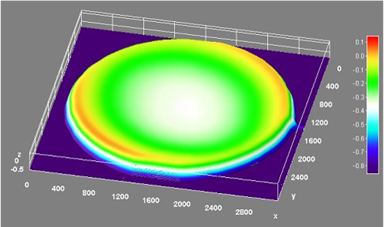
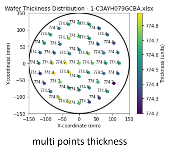
Warpage & Thickness Measurement
Key Indicators
- TTV (Total Thickness Variation): difference between max and min thickness
- Bow: overall wafer bending relative to a reference plane
- Warp: global deformation including local undulation
- Flatness: deviation from best-fit reference plane
Outputs include wafer maps, statistical plots, extreme point markers, and heatmaps for yield monitoring.
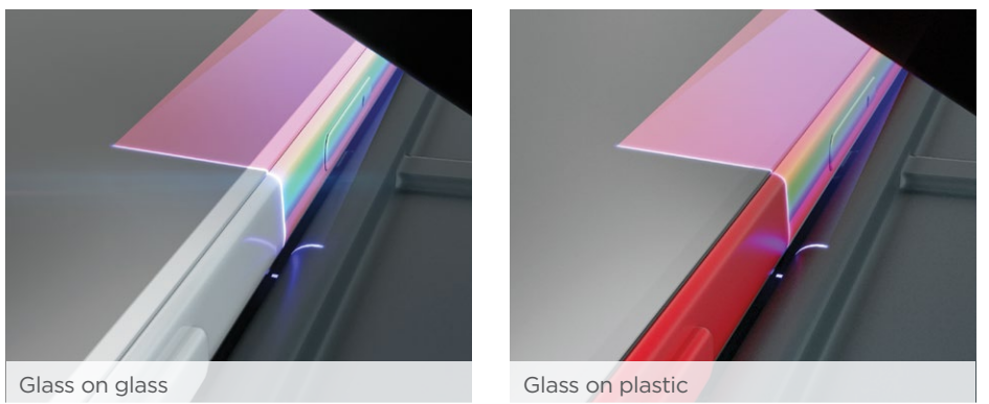
Layered/Regional Thickness
For multilayer structures such as Glass on Glass/Plastic, we provide localized thickness, step height, and profile analysis with ROI-based reporting.
- Multiple ROIs and grid sampling
- Cross-section/profile extraction tools
- Automated batch reporting (CSV/PDF/images)
Decision Guide
Three key questions to select the right approach:
- Sample attributes: Transparent? Highly reflective? Feature size?
- Metrics needed: Thickness, TTV, Bow, Warp, Flatness, GD&T?
- Throughput/coverage: Full-field or ROI? One-off or inline sampling?
We provide sample evaluation reports recommending optical setup, fixturing, scanning strategy, and output formats.
Calibration & Measurement Uncertainty
Traceable Calibration
Reference standards (step height, flatness, spheres) are used to establish calibration routines. Environmental monitoring (temperature/vibration) ensures long-term stability.
- Reference sample management
- Scheduled recalibration and records
- Recipe version control and sign-off
Uncertainty & Risk Control
Comprehensive uncertainty analysis covers repeatability, reproducibility, systematic error, and operator variation. Reports help define practical tolerances for incoming/outgoing QC.
Results are documented with key environment/fixturing parameters for traceability.
Workflow & Output
- Pre-measurement: fixturing, condition check, cleaning, marking
- Measurement: single-point/mesh scans, real-time QC
- Analysis: point cloud cleaning, meshing, statistics, CAD comparison
- Output: CSV, PDF, STL/PLY/OBJ, heatmaps, wafer-maps
- Integration: optional MES/PLM/cloud connectivity
Applications
- Wafer TTV/Bow/warpage monitoring for process optimization
- Glass stacks (GoG/GoP) thickness and flatness inspection
- GD&T of exterior components: edge, hole, assembly fit
- Coating thickness, step height, and defect analysis
- Assembly interference prediction (gap/interference analysis)
- Incoming/outgoing inspection and supply chain consistency
- R&D DOE: correlating surface metrics with reliability
- Automotive display and consumer optics mass-production QC
FAQ
- Q1: Can high-reflective samples be measured?
Yes, with proper strategies (polarization, aperture, angles, multiple scans). Optimized during evaluation. - Q2: What is the achievable accuracy?
Depends on material, roughness, environment, fixturing. Trial runs yield statistical results and uncertainty reports. - Q3: Can it integrate with CAD/PLM?
Yes, exports common 3D formats and batch reports; custom APIs available if required. - Q4: How is throughput planned for production?
We balance sampling density.