
APPLICATION

- Home
- Application
- Integrated Wafer and Thin Film Metrology Solutions
- Integrated Wafer and Thin Film Metrology Solutions
Integrated Wafer and Thin Film Measurement Solutions
TTV ・ Warpage ・ Multi-layer Thickness ・ 3D Topography ・ Roughness
From nm to mm: A One-Stop Measurement Solution
About iBoson: From Sensors to Turnkey Systems
iBoson Technology specializes in optical measurement system integration, combining various interferometry, spectroscopy, and ellipsometry technologies. We customize measurement solutions based on customer material and process requirements, ready for direct deployment in both R&D and production lines.
Technology Selection
Select the most suitable technology combination based on material, thickness, and precision requirements.
System Integration
Seamless integration of measurement probes, stages, fixtures, and software.
Algorithm & Analysis
TTV / Warp / Thickness Mapping, and SPC reporting.
Local Service
Sample evaluation, acceptance testing, training, and warranty support.
Industry Challenges: Thinner Wafers and Complex Structures Elevate Measurement Difficulty
Wafer Level
- Thinning down to the 20 µm level causes larger warpage.
- LN / LT piezoelectric wafer heterogeneous bonding (glass, silicon, sapphire).
- Opaque metal coatings prevent single-sided optical penetration.
- High-doped Si causes strong absorption and NIR signal attenuation.
Thin Film Level
- Simultaneous determination of n, k, and thickness at the nanoscale.
- Layer-by-layer resolution required for multi-layer stacks.
- Micro-area (≤ 30 µm) measurement for patterned wafers.
- Full-wafer mapping for thickness uniformity.
Production Line Level
- Measurement speed must match process Takt time.
- High repeatability and long-term stability.
- Non-contact and non-destructive to samples.
- Data must integrate seamlessly with SPC / MES.
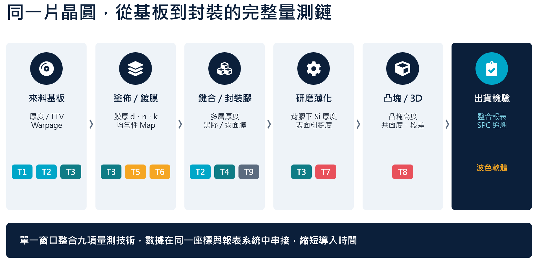
Nine Core Measurement Technology Codes
| Code | Technology Name | Key Measurement Items | Application Features |
|---|---|---|---|
| T1 | IR White Light Interferometry | Wafer Thickness・TTV | Wafer Geometry |
| T2 | Multi-peak Interferometric Displacement | Multi-layer Thickness+Warpage | Thick Film / Si / Haze |
| T3 | Broadband Spectral Interferometry | Si Penetration・Coated Films | Thin Film Optics |
| T4 | High-penetration Spectral Interferometry | Haze Films・EMC・Thick Films | Thick Film / Si / Haze |
| T5 | Reflectance Spectroscopy | Thin Film d・n・k・Map | Thin Film Optics |
| T6 | Spectroscopic Ellipsometry | Ultra-thin Films・Precise n/k | Thin Film Optics |
| T7 | Monochromatic Light Interferometry | Surface Roughness | Surface Topography |
| T8 | Line Confocal 3D Scanning | 3D Topography・Bumps・Steps | Surface Topography |
| T9 | Dual-probe Caliper Measurement | Opaque Wafer Thickness | Opaque Materials |
Selection Guide: Three Steps to Determine Measurement Technology
- STEP 1: What to measure? Thickness / TTV, Warpage; Multi-layer thickness; Film thickness & n, k; 3D topography / Roughness.
- STEP 2: Material optical properties? Transparent (Glass, LN, Sapphire); Si (Requires SWIR IR band); Haze / EMC (High scattering); Metal coatings (Opaque).
- STEP 3: Thickness of each layer? ≥ 10 µm → T2; 0.3–10 µm → T3; 10 nm–several µm → T5; < 100 nm → T6.
Example: LN 20 µm bonded to glass, measuring TTV+Warpage → Transparent → ≥ 10 µm per layer → T2 Multi-peak Interferometric Displacement, completed with a single probe.
By Material Type: Technology Overview
| Material | Optical Properties | Recommended Tech | Notes |
|---|---|---|---|
| Glass / Quartz | Transparent | T2・T1・T3・T5 | — |
| Sapphire | Transparent | T2・T1 | — |
| LN / LT Piezo Wafers | Transparent | T2・T1 | X / Y-cut double refraction, sample evaluation recommended. |
| Si Wafers / Thinned Wafers | Opaque at 840 nm | T3 (SWIR 40–775 µm, penetrates backing tape)・T1 (1100 nm) | T1 is used for high-doped Si. |
| SiO₂ / SiN Dielectric Films | Transparent | T5・T6 | Prioritize T6 for < 100 nm. |
| Photoresist / PI / Organic Films | Transparent to Translucent | T3・T5・T6 | Requires optical model establishment. |
| Haze Films / EMC / Composite Films | High scattering / Absorption | T4 (Penetrates ~1 mm EMC) | Max total thickness ≤ 3 mm, resolves up to 3 layers. |
| Metal Coatings / Opaque | Opaque | T9 (Thickness)・T8 / T7 (Surface) | Requires standard wafer for probe gap calibration. |
| Bumps / Microstructures | 3D Structure | T8 (3D Topography)・T3 Microscopic (Thickness) | — |
By Measurement Item: Technology Mapping
| Measurement Item | Wafer Thickness / TTV | Warpage / Bow / Warp | Multi-layer Thickness | Thickness+Refractive Index n, k | Haze Film / EMC Thickness | 3D Topography / Bumps / Steps | Surface Roughness Ra / Rz |
|---|---|---|---|---|---|---|---|
| T1 IR White Light Interferometry | Primary | Primary | Conditional | ||||
| T2 Multi-peak Interferometric Displacement | Primary | Primary | Primary | ||||
| T3 Broadband Spectral Interferometry | Primary | Conditional | Primary | Primary | |||
| T4 High-penetration Spectral Interferometry | Conditional | Conditional | Primary | Primary | |||
| T5 Reflectance Spectroscopy | Primary | Primary | |||||
| T6 Spectroscopic Ellipsometry | Conditional | Primary | |||||
| T7 Monochromatic Light Interferometry | Conditional | Primary | |||||
| T8 Line Confocal 3D Scanning | Conditional | Primary | Conditional | ||||
| T9 Dual-probe Caliper Measurement | Primary |
Note: For transparent wafers requiring simultaneous thickness+warpage measurement → T2; For haze films / EMC → T4
Technical Specifications Quick Reference
Specifications vary depending on material, refractive index, and specific models; subject to actual sample evaluation results.
| Technology | Primary Application | Measurement Range | Accuracy / Resolution | Spot Size / FOV | Speed |
|---|---|---|---|---|---|
| T1 IR White Light Interferometry | Wafer Thickness / TTV | 1 µm–1.4 mm (Glass); Si 50 µm–1.05 mm | Resolution < 1 nm; Linearity ±0.1 µm | Point measurement | 6 kHz |
| T2 Multi-peak Interferometric Displacement | Multi-layer Thickness+Warpage | Z 2.1 mm; 10 µm–1.3 mm per layer, ≤ 13 layers | Resolution 30 pm–1 nm; Linearity ±10–50 nm | 10 µm | 6 kHz |
| T3 Broadband Spectral Interferometry | Si Thickness / Coated Films | Si 40–775 µm; Film 0.3–200 µm | CV < 0.1%; Resolution 0.001–0.01 µm | 10 µm–1 mm | < 1 s / point |
| T4 High-penetration Spectral Interferometry | Haze / EMC / Thick Films | 50 µm–3 mm (n=2), up to 3 layers | Resolution 0.1 µm; Repeatability ≤ 0.5 µm | 2 mm (WD 90 mm) | 1 s / point |
| T5 Reflectance Spectroscopy | Thickness, n, k, Map | 10 nm–350 µm (Depending on band) | Accuracy < 2 nm or 0.2%; Stability 0.1 nm | 10–30 µm (Microscopic) | 12-inch Auto Map |
| T6 Spectroscopic Ellipsometry | Ultra-thin Films, n, k | nm-level Films | Δ, Ψ < ±0.3%; Thickness / n, k < ±0.3% | Incident angle 45–90° | — |
| T7 Monochromatic Light Interferometry | Surface Roughness | Height 1–160 nm | Ra Repeatability ±0.5 nm | 1.6 × 1.3 mm | 2 s |
| T8 Line Confocal 3D Scanning | 3D Topography / Bumps | Line length 7 mm (2,624 pts); Z 2.1 mm | Z Resolution 200 nm; Lateral 2.7 µm | Line profile | 10 kHz profile |
| T9 Dual-probe Caliper Measurement | Opaque Wafer Thickness | Depends on probe configuration | Depends on probe; Standard wafer calib. | 10 µm | 6 kHz |
Integrated Measurement Workflow & System Architecture
- iBoson Measurement Software: Recipe management, auto-patterning (polar/rectangular/linear), Map visualization, SPC, reporting, MES interface.
- Measurement Probes (Optional): T1–T9 interferometry, spectroscopy, ellipsometry, line confocal, and dual-probe configurations.
- Motion & Positioning: XY / R-θ / Z stages, auto-focus, vision alignment, granite base.
- Stages & Fixtures: Vacuum chucks, 3-point support, 4–12 inch wafer fixtures, dual-probe calipers.
The same platform can be equipped with multiple probes as needed, sharing identical recipes and data formats for both R&D validation and mass production deployment.
Partnership Process: From Sample Evaluation to Mass Production, iBoson Supports You Every Step of the Way
STEP 1 Requirements Interview
Materials, dimensions, specs, and takt time.
Materials, dimensions, specs, and takt time.
STEP 2 Sample Evaluation
Empirical testing to verify technical feasibility.
Empirical testing to verify technical feasibility.
STEP 3 Feasibility Report
Measurement data and solution recommendations.
Measurement data and solution recommendations.
STEP 4 Custom Design
Quotation, mechanical, and software planning.
Quotation, mechanical, and software planning.
STEP 5 Acceptance & Training
Installation, MSA, training, and warranty.
Installation, MSA, training, and warranty.
Make Measurement Your Process Competitive Advantage
-----------------------------------------------------
We welcome you to provide samples for empirical evaluation by iBoson. Please provide: materials and structures, wafer sizes, thickness ranges, target specifications, measurement takt time, and application scenarios.